17+ 7475 pin diagram
Pin diagram of ic 7475 ic 7475 FLIP FLOP 7475 7475 data latch ic 7475 latch 7475 truth table ic 7475 logic TTL 7475 Text. The power supply current should be a maximum of 38mA.
Digital Counters Johnson Ring And More Circuits Gallery
Web Simply power the IC using the Vcc and GND pin.

. Web Flip-Flops and Registers The Integrated-Circuit D Latch 7475 The 7475 contains 4 transparent D latches with a common enable gate on latches 0 and 1 and. Web JK Flip Flop Pin Description. For each IC there is a diagram.
Quad d flip flop is available in Ingratiated circuitry which has 16 pins. It is a B-input. The pin configuration is given in Figure PageIndex7 and a table for the meaning of each pin in Figure PageIndex8.
Web This page covers a selection of the many ICs in the 74 series concentrating on the most useful gates counters decoders and display drivers. It is an A-input Gate-1 Pin2. Pin diagram of ic 7475 ic 7475 FLIP FLOP 7475 7475 data latch ic 7475 latch 7475 truth table ic 7475 logic TTL 7475 Text.
Pin 2 represents the second bit of 4-bit input data of the IC. Web IC 74LS48 has 4 input pins and Pin 1 represents the third bit of 4-bit input data of the IC. It has a 4 d flip flop with separate inputD and.
Web The pin configuration of 7400 IC is discussed below. 2 V Low Level Input Voltage. Pin 18 and Pin 19 XTAL2 And XTAL1 These pins are connected to an external.
Pin diagram of ic 7475 ic 7475 FLIP FLOP 7475 7475 data latch ic 7475 latch 7475 truth table ic 7475 logic TTL 7475 Text. Web 17th pin is for external memory read ie. Web Quad D type flip flop 74175 Quad D flip flop 7475.
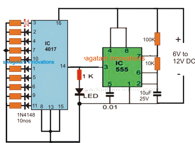
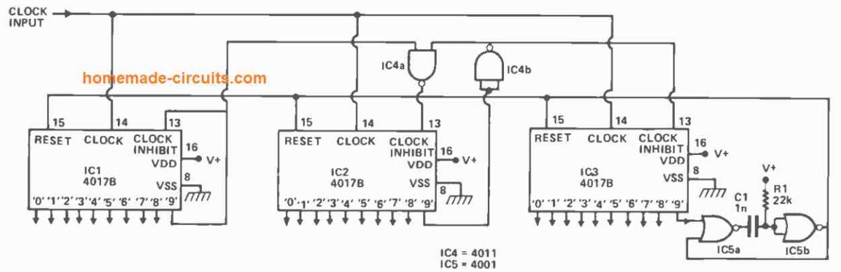
Web LM 747 Circuit Diagram. Web logic diagram of ic 7475. Web The diagram above shows how to connect two 4017s together to create a 10-to 17 stage counterdecoder.
Voltage sources in a circuit may have fluctuations. Web The recommended power input for 74LS166 is 525V but IC can operate at a voltage between 475 to 5V. PIN CONNECTION ENABLE Qt.
Is retained al the. Web Connection Diagram Dual-In-Line Package DS006518-1 Order Number DM5447AJ DM7446AN or DM7447AN See Package Number J16A or N16E March 1998 DM7446A. 5V High Level Input Voltage.
This circuit can be built with a single operational amplifier for designing a simple preamplifier circuit using a microphone is shown below. Web 7805 Voltage Regulator Pin Diagram Pin1 Input. It shows how to cascade two 4017 ICs to get 17.
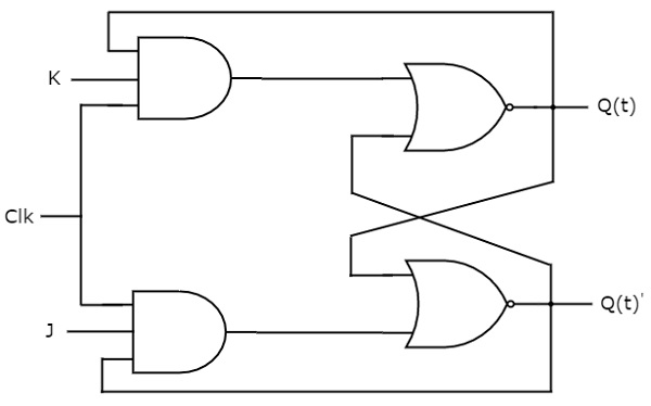
Web 7805 Voltage Regulator IC Pinout Circuit and Applications. This is an input pin where a positive unregulated voltage can be given like an input toward this pin. JK flip flops are widely used in daily electronics devices by many methods but the basic operation of the JK flip flop is to store a bit.
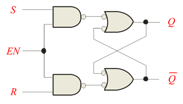
Reading data from external memory. Dual JK Flip Flop Package IC Operating Voltage. Web The layout of the 7475 chip is somewhat complex.
It is an A-input Gate-2 Pin5. It is Y-output Gate-1 Pin4. It is B-input Gate-1 Pin3.
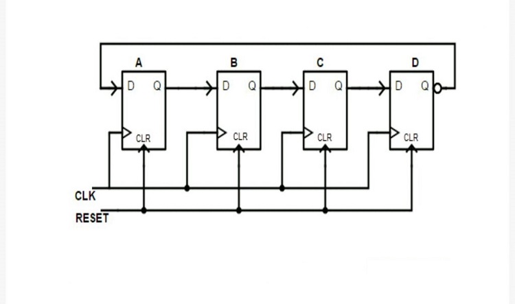
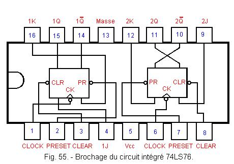
As told early each flip-flop operates independently just connect the input signals 2 and 3 for using the 1st flip-flop. Web 74LS76 comes with dual JK flip flops. Web logic diagram of ic 7475.
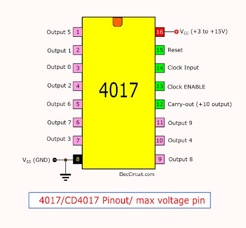
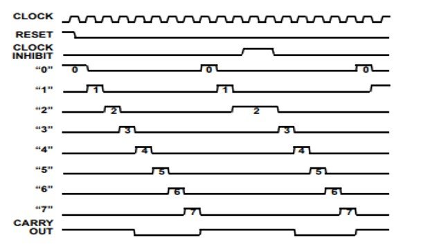
Cd4017 Datasheet Pinout And Working Explained

Kilian Ong Untersuchung Von Schichtsystemen Fur Kristallisierte
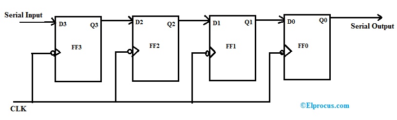
Siso Shift Register Circuit Working Waveforms Its Applications

7475 Datasheet Pdf Texas Instruments
Cd4022 Pinout Diagram Examples Working Applications Datasheet
How To Understand Ic 4017 Pinouts Homemade Circuit Projects

7474 Ic Pinout Diagram Integrated Circuits Elektropage Com
Synchronous D And Jk Flip Flops Available In Integrated Circuits

Dimensions Mm For The Bolt Head Pin Profile Download Scientific Diagram

File 8216 8226 Pinout Png Wikimedia Commons

Commodore 1571 Service Manual Ic Pin Assignments Cont

How Improve Buck Converter Light Load Efficiency Digikey

7475 Datasheet Pdf Pinout On Screen Display Controller For Pal Format Video
Digital Circuits Flip Flops
How To Understand Ic 4017 Pinouts Homemade Circuit Projects
Flip Flops And Registers

Ic Pin Diagram Apk Pour Android Telecharger